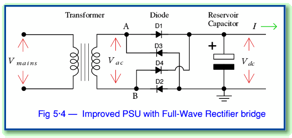
The simple arrangement shown in figure 5·1 isn’t particularly effective. There are a range of other, more complex arrangements which provide a more stable d.c. level or more power. Here we will just look briefly at a few of the many improvements that can be made. The first, and most common of these is the use of a Full-Wave Rectifier Bridge. This is shown in figure 5·4. Comparing figure 5·4 with 5·1 we can see that the change is that we now use four diodes instead of one. These diodes act to ‘steer’ the input as follows:
As with the simple arrangement, the reservoir capacitor is charged whenever the input a.c. is large enough. However this can now happen in two ways which we can understand by considering the relative voltages,  and
and  at the two points, ‘A’ and ‘B’ shown on figure 5·4
- When
 we will find that
  . This permits the pair of diodes, D1 & D2, to conduct, thus recharging the capacitor.
- When
 we will find that
  . This permits the pair of diodes, D3 & D4, to conduct, recharging the capacitor.
The result is the capacitor can now be recharged twice during every input a.c. cycle. So when the input is a 50Hz sinewave we recharge and ‘top up’ the capacitor’s voltage 100 times per second (i.e. every 10 milliseconds). This is better than the simple one diode supply which can only top up the reservoir every 20 milliseconds. Since the time between recharges is halved we can expect the amplitude of the ripple to be halved. Hence the result is a smoother d.c. output. Since diodes are quite cheap, it is usual to use a full-wave rectifier. The only drawback is that the charging current flowing from the transformer to the capacitor now has to pass through two diodes in series. Hence the ‘drop’ in voltage lost across the diodes is doubled from around 0·5 V to about 1 V.
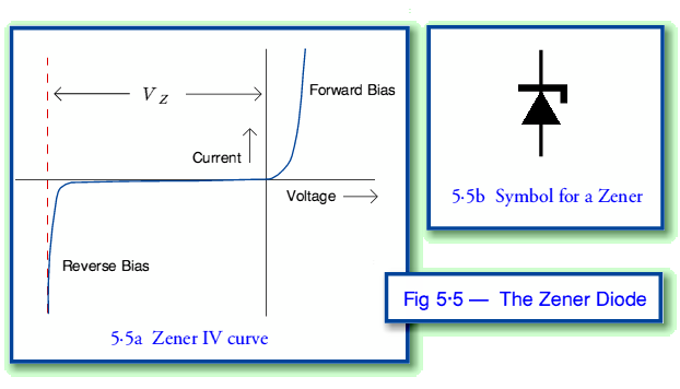
The second commonly employed improvement is the use of a Zener Diode, or some similar device. The Zener has a typical IV curve whose shape is shown in figure 5·5a. The device is engineered to suffer a ‘breakdown’ when a large enough reverse bias voltage is applied. By suitable semiconductor design and manufacturing the voltage at which this occurs can be set for a specific diode to be at almost any level,  , from around a couple of volts to many tens of volts. The breakdown can be quite ‘sharp’. As a result we can approximate the Zener’s properties in terms of three rules:
- – In forwards bias (not normally used for a Zener) the behaviour is like an ordinary semiconductor diode.
- – In reverse bias at voltages below
 the device essentially refuses to conduct, just like an ordinary diode.
- – In reverse bias, any attempt to apply a voltage greater than
 causes the device to be prepared to conduct a very large current. This has the effect of limiting the voltage we can apply to around
  .
.
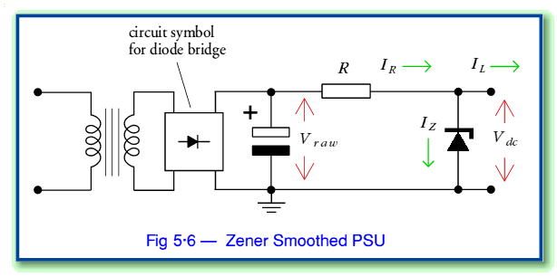
We can therefore build a circuit of the kind shown in figure 5·6 and use it to suppress power line voltage variations. Note that in this circuit I have used the standard symbol for a full-wave diode rectifier bridge. This arrangement of four diodes is so commonly used that it can be bought with the four diodes in a single package and has its own symbol as shown.
The effect of the Zener in this circuit can be explained as follows. Let us assume that the d.c. level,  , provided by the bridge and reservoir capacitor is greater than the chosen Zener’s breakdown voltage,
  . This means that the series resistor will see a potential difference between its ends of
  and we find that the output voltage,
  almost irrespective of the choice of the resistor value,
  , and of
  . When no load current,
  , is being drawn by anything connected to the supply, we find that the current through the resistor and hence the Zener will therefore be
Now consider what happens when the attached load draws a current in the range 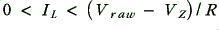 . In effect, the current arriving via the resistor,
  , is now ‘shared’ by the Zener and the load. This means that there will still be a non-zero current for
  , hence it maintains the output level at about
 . As a result, provided we don’t attach a load that tries to draw a current larger than
  , the voltage across the Zener will be ‘held’ at the same value,
 . In practice, the action of the Zener is just to draw whatever current is required in order to ensure that the voltage drop across
  will be whatever is needed to ensure that the voltage across the Zener is
Looking back at Figure 5.5 can see that the Zener does not actually maintain exactly the same voltage when we allow the current it takes to vary, but the variation is relatively small provided we ensure the Zener current does not fall too close to zero. When designing a Zener controlled PSU in more detail we could use a value for the dynamic resistance of the chosen Zener in order to take this into account. This dynamic resistance value is a measure of the slope of the reverse bias breakdown part of the curve shown in figure 5.5. Lists of components will generally give a value for this resistance as well as the nominal Zener voltage, and power handling, for each Zener diode. We would then use this data to select the Zener required for a given purpose.