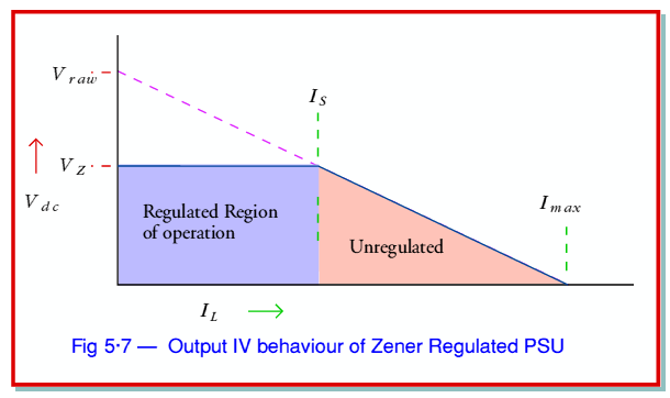
If we allow the current drawn by the load to exceed the current level set by expression 5.12 the situation will change. Once  there will be “no current left over” for the Zener to draw. In this situation the zener has no effect. The current demanded by the load must come via the resistor,
  . Hence we now have a situation where the current through the resistor will be
  and have a value greater than the value of
  we would calculate from expression 5.12. From Ohm’s Law. this increase in resistor current means that the voltage across the resistor must now exceed
  . Unless we have arranged for the input,
  , to rise, this means that
  must now be less than
  . Any further increase in the current demanded by the load causes a further fall in the output voltage. As a result, at these high load currents the zener has no effect and we just see the system behaving in a way set by the presence of the resistor,
  , in series with the raw d.c. level. The overall behaviour can be represented by the graph shown in figure 5·7.
We can divide the operation into two areas – regulated and unregulated. In the regulated area the output voltage is controlled by the action of the Zener, and in the unregulated region it is not. In the regulated region we have
where  represents the maximum regulated current value
and the maximum possible available unregulated current is
In principle, a Zener regulated supply works well provided that we do not attempt to demand a load current greater than  . Within limits, it permits us to hold a steady output level even when the demanded current varies. It also tends to ‘reject’ any ripple. A small change in the voltage,
  , will alter the value of
  by a corresponding amount. However provided that
  always remains greater than the current demanded by the load, the Zener will still take some current and effectively hold the output voltage at a steady level. Hence the Zener helps to suppress unwanted ripple. Although very useful, the circuit shown in Figure 5.6 does have one serious drawback in situations where we require a significant output voltage and current. As an example to illustrate this, consider a situation where we require an output
  of 15 Volts and have to supply load currents at this voltage up to 2 Amps.
In order to ensure we can bias the system we can choose a value of  a few volts greater than 15 V – lets take
  of 20 Volts for the sake of example. Since we require currents up to 2 Amps we have
  . Using expression 5.15 this means we must choose a resistor,
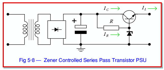
  . The first consequence of the way the circuit works is that the resistor always has to pass a current of at least 2 Amps, so must dissipate 5 Watts even when no output is required. The second consequence is that when no output (load) current is demanded all of this current then passes though the Zener, hence meaning it has to dissipate 15 × 2 = 30 Watts! This indicates that the arrangement shown in figure 5·6 suffers from the ‘Class A problem’. i.e. It has a relatively large quiescent current and power dissipation level. The cure for this is actually quite simple. We can add a Series Pass transistor as shown in figure 5·8.
Here the output from the resistor-Zener combination isn’t used to directly supply the load current. Instead, it sets the voltage on the base of an output transistor. This means that when a given maximum current,  , is required by the load, the resistor-Zener only have to supply a maximum current of
  where
where  is the current gain of the transistor. Given, say, a transistor with a current gain value of ×100 this means the quiescent current required through the resistor and Zener fall by a factor of 100. i.e. We now only need to pass 20 mA through the resistor and Zener to have a power supply capable of providing up to 2 Amps at a regulated voltage. The result is that the quiescent power dissipation in the PSU is 100 times lower than previously. Now, the transistor only passes the required current (and dissipates power) as and when the attached load demands it.
The above design is considerably more power efficient and practical than the simple Zener system. However it does suffer from the drawback that there is an extra ‘diode drop’ in the way due to the base-emitter junction between the Zener and the output. This needs to be taken into account when designing a PSU for a specific output voltage. Most real PSU circuits are more complex than is shown in figure 5·8 but the extra complications are usually designed to improve specific aspects of the performance and the operation is basically as explained above. There are in fact a wide range of types of PSU including ‘Switched Mode’ types. Each have their particular good and bad points. However circuits of the type outlined above generally work well in simple cases where a reliable PSU is required.
Summary
You should now understand how the combination of a rectifier diode and a reservoir capacitor can be used to obtain a d.c. level from and a.c. input. How a transformer can be used to step up or down the a.c. level, and hence choose the desired size of input to the diode bridge. You should also know how a Full-Wave Rectifier Bridge improves performance by doubling the number of recharging opportunities per input a.c. cycle. You should also now understand how a Zener Diode can be used to Regulate the d.c. level and reduce any ripple and that the use of a Series Pass Transistor can improve the power efficiency and capability of the PSU.


