2.2 Class A
The circuit illustrated in Figure 2·1 and discussed in the previous section is an example of a Class A amplifier stage. Class A amplifiers have the general property that the output device(s) always carry a significant current level, and hence have a large Quiescent Current. The Quiescent Current is defined as the current level in the amplifier when it is producing an output of zero. Class A amplifiers vary the large Quiescent Current in order to generate a varying current in the load, hence they are always inefficient in power terms. In fact, the example shown in Figure 2·1 is particularly inefficient as it is Single Ended. If you look at Figure 2·1 again you will see that the amplifier only has direct control over the current between one of the two power rails and the load. The other rail is connected to the output load through a plain resistor, so its current isn’t really under control.
We can make a more efficient amplifier by employing a Double Ended or Push-Pull arrangement. Figure 2·3 is an example of one type of output stage that works like this. You can see that this new arrangement employs a pair of transistors. One is an NPN bipolar transistor, the other is a PNP bipolar transistor. Ideally, these two transistors have equivalent properties – e.g. the same current gains, etc – except for the difference in the signs of their voltages and currents. (In effect, a PNP transistor is a sort of electronic “mirror image” of an NPN one.)
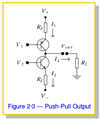
The circuit shown on the left now has two transistors which we can control using a pair of input voltages,  and
and  . We can therefore alter the two currents,
  and
and  independently if we wish.
In practice, the easiest way to use the circuit is to set the Quiescent Current,  to half the maximum level we expect to require for the load. Then adjust the two transistor currents ‘in opposition’.
It is the imbalance between the two transistor currents that will pass through the load so this means the transistors ‘share’ the burden of driving the output load.
When supplying a current,  to the load this means that we will have
In linear operation this limits us to a current range  in each transistor, and load currents in the range
  . Hence this arrangement is limited in a similar way to before. However the important difference to before becomes clear when we take the same case as was used for the previous example, with
  power lines and a
  load.
load.
Since we wish to apply up to 25 V to a  load we require a peak output load current of 2·5 Amps. This means we can choose
  . As a result, each transistor now only has to dissipate 1·25 × 25 = 31 Watts – i.e. the output stage dissipates 62 Watts in total when providing zero output. Although this still isn’t very efficient, it is rather better than the value of well above 1 kW required for our earlier, single ended, circuit!
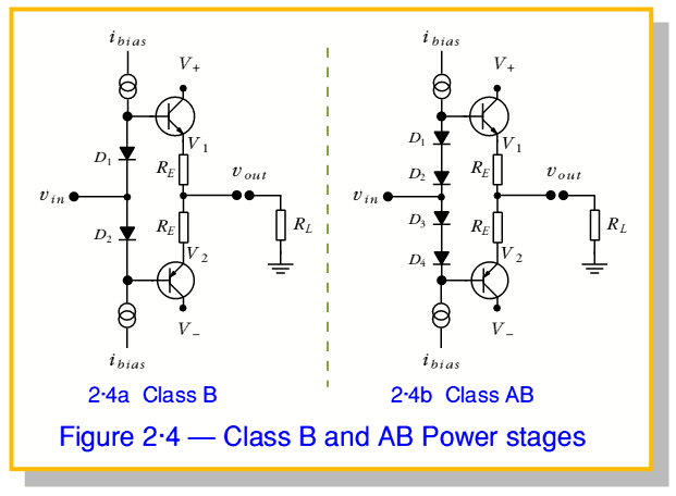
2·3 Class B
Note that as is usual in electronics there are a number of arrangements which act as Class A amplifiers so the circuit shown in Figure 2·3 is far from being the only choice. In addition we can make other forms of amplifier simply by changing the Quiescent Current or Bias Level and operating the system slightly differently. The simplest alternative is the Class B arrangement. To illustrate how this works, consider the circuit shown in Figure 2·4a. Once again this shows a pair of devices. However their bases (inputs) are now linked by a pair of diodes.
The current in the diodes is mainly set by a couple of constant current stages which run a bias current,  , through them. If we represent the forward voltage drop across each diode to be
  we can say that the input to the base of the upper transistor sits at a voltage of
  , and the input to the base of the lower transistor sits at
  . Now since the base-emitter junction of a bipolar transistor is essentially a diode we can say that the drop between the base and emitter of the upper transistor will also be
  . Similarly, we can say that the emitter of the lower (PNP) transistor will be
  above its base voltage.
This leads to the very interesting result where the emitter voltages in 2·4a will be
This has two implications. Firstly, when  the output voltages will be zero. Since this means that the voltages above and below the emitter resistors (
 ) will both be zero it follows that there will be no current at all in the output transistors. The Quiescent Current level is zero and the power dissipated when there is no output is also zero! Perfect efficiency!
The second implication is that as we adjust  to produce a signal, the emitter voltages will both tend to follow it around. When we have a load connected this will then draw current from one transistor or the other – but not both. In effect, when we wish to produce an positive voltage the upper transistor conducts and provided just enough current to supply the load. None is wasted in the lower transistor. When we wish to produce a negative voltage the lower transistor conducts and draws the required current through the load with none coming from the upper transistor. Again this means the system is highly efficient in power terms.
This all seems to be too good to be true, there must be a snag... and yes, there are indeed some serious drawbacks. When power efficiency is the main requirement then Class B is very useful. However to work as advertised it requires the voltage drops across the diodes and the base-emitter junctions of the transistors to all be exactly the same. In practice this is impossible for various reasons. The main reasons are as follows:
- No two physical devices are ever absolutely identical. There are always small differences between them.
- The diodes and the transistors used will have differently doped and manufactured junctions, designed for different purposes. Hence although their general behaviours have similarities, the detailed IV curves of the transistor base-emitter junctions won’t be the same as the IV curves of the diodes.
- The current through the transistors is far higher than through the diodes, and comes mostly from the collector-base junctions which are intimately linked to the base-emitter. Hence the behaviour is altered by the way carries cross the device.
- The transistors will be hotter than the diodes due to the high powers they dissipate. Since a PN junction’s IV curve is temperature sensitive this means the transistor junctions won’t behave exactly like the diodes, and may change with time as the transistor temperatures change.
- When we change the applied voltage it takes time for a PN junction to ‘react’ and for the current to change. In particular, transistors tend to store a small amount of charge in their base region which affects their behaviour. As a result, they tend to ‘lag behind’ any swift changes. This effect becomes particularly pronounced when the current is low or when we try to quickly turn the transistor “off” and stop it conducting.
The overall result of the above effects is that the Class B arrangement tends to have difficulty whenever the signal waveform changes polarity and we have to switch off one transistor and turn on the other. The result is what is called Crossover Distortion and this can have a very bad effect on small level or high speed waveforms. This problem is enhanced due to Non-Linearities in the transistors – i.e. that the output current and voltage don’t vary linearly with the input level – which are worst at low currents. (We will be looking at signal distortions in a later section.)
This places the amplifier designer/user in a dilemma. The Class A amplifier uses devices that always pass high currents, and small signals only modulate these by a modest amount, avoiding the above problems. Alas, Class A is very power inefficient. Class B is far more efficient, but can lead to signal distortions. The solution is to find a ‘half-way house’ that tries to take the good points of each and minimise the problems. The most common solution is Class AB amplification, and an example of this is shown in Figure 2·4b.