Every real amplifier has some unavoidable limitations on its performance. The main ones that we tend to have to worry about when choosing and using them are:
- Limited bandwidth. In particular, for each amplifier there will be an upper frequency beyond which it finds it difficult/impossible to amplify signals.
- Noise. All electronic devices tend to add some random noise to the signals passing through them, hence degrading the SNR (signal to noise ratio). This, in turn, limits the accuracy of any measurement or communication.
- Limited output voltage, current, and power levels. This will mean that a given amplifier can’t output signals above a particular level. So there is always a finite limit to the output signal size.
- Distortion. The actual signal pattern will be altered due non-linearities in the amplifier. This also reduces the accuracy of measurements and communications.
- Finite gain. A given amplifier may have a high gain, but this gain can’t normally be infinite so may not be large enough for a given purpose. This is why we often use multiple amplifiers or stages to achieve a desired overall gain.
Let’s start by looking at the limits to signal size.
2.1 Power Limitations
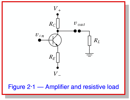
Figure 2·1 shows a simple amplifier being used to drive output signals into a resistive load.
The amplifier is supplied via power lines at  and
and  so we can immediately expect that this will limit the possible range of the output to
  as the circuit has no way to provide voltages outside this range. In fact, the output may well be rather more restricted than this as we can see using the following argument.
In effect, we can regard the transistor as a device which passes a current whose level is primarily determined by its base-emitter voltage, and hence by the input,  . However any current it draws from its collector must pass through
  or
or  , and any current emerging through its emitter must then flow through
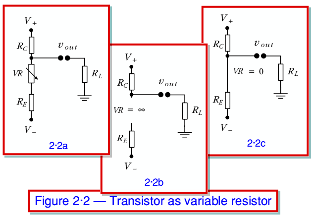
  . In practice it really acts a sort of ‘variable resistor’ placed in between these other resistors. We can therefore represent it as being equivalent to the circuit shown in Figure 2·2a where the transistor is replaced by a variable resistance, VR.
When we lower the input voltage,  , we reduce the transistor’s willingness to conduct, which is equivalent to increasing its effective collector-emitter resistance. Taking this to the most extreme case we would reduce the current it passes to zero, which is equivalent to giving it an effective collector-emitter resistance of infinity. This situation is represented in figure 2·2b. Alternatively, when we increase
  we encourage the transistor to pass more current from collector to emitter. This is equivalent to reducing its effective collector-emitter resistance. Again, taking this to the extreme we would reduce its resistance to zero as shown in 2·2c. We can now use the extreme cases shown in 2·2b and 2·2c to assess the maximum output the circuit can provide, and the implications for the design.
From 2·2b we can see that the highest (i.e. most positive) current and voltage we can provide into a load,  , will be
as the collector resistor acts a a Potential Divider with the load to limit the fraction of the available positive power line voltage we can apply to the output. Looking at expressions 2.1 and 2.2 we can see that we’d like  to enable the maximum output to be able to be as big as possible – i.e. to approach
  . For the sake of example, lets assume that we have therefore chosen a value for
  equal to
  .
.
Now consider what happens when we lower the transistor’s resistance (i.e. increase the current it will conduct) to the maximum case shown in 2·2c. We now find that the minimum (most negative) output voltage and current will be
where we can define
Either by considering the diagram or examining these equations we can say that in order for  to be able to approach
  we require
  (where
  represents the value of the parallel combination). Since we have already chosen to set
  this is equivalent to choosing a value of
  . Again, we can assume for the sake of example that
  is chosen to be
  which means it will also apprimate to
  .
.
To consider the implications of the above lets take a practical example based on a power amplifier for use as part of an audio system. This means we can expect  to be of the order of 8 Ohms. For simplicity, lets assume
  . Following the assumptions above this means we would choose
  and
and  . Again, for the sake of example, lets assume that the voltage rails available are
  . This would mean that for an ideal amplifier we could expect to output peak levels of about 90% of
  which for a sinewave would correspond to about 30 Watts rms maximum power delivered into the
  load.
load.
Now consider what happens when the amplifier is on, but isn’t trying to deliver a signal to the load – i.e. when  . This means that there will be 25 Volts across
  . Since this has a resistance of
  it follows that
  when
when  . i.e. the amplifier will demand 25 Amps from its positive power supply. Since none of this is being sent to the load this entire current will be passed through the transistor and its emitter resistor and away into the negative power rail supply. The result is that 25 × 50 = 1250 Watts will have to be dissipated in the combination of
  , the transistor, and
  in order to supply no actual output!
It would be fair to describe this kind of design as being “quite inefficient” in power terms. In effect it will tend to require and dissipate over 1 kW per channel if we wanted to use it as a 30 Watt power amplifier. This is likely to require large resistors, a big transistor, and lots of heatsinks. The electricity bill is also likely to be quite high and in the summer we may have to keep the windows open to avoid the room becoming uncomfortably warm. Now we could increase the resistor values and this would reduce the “standing current” or Quiescent Current the amplifier demands. However it would also reduce the maximum available output power, so this form of amplifier would never be very efficient in power terms. To avoid this problem we need to change the design. This leads us to the concept of amplifier Classes.