8·1 Op Amp Circuits
Operational Amplifier ICs are very widely used in analog signal processing systems. Their obvious use is as amplifier, however they can be used for many other purposes – for example in the active filters we considered in part 3 of the series of pages on Analog and Audio. This section looks at the basic way Op-Amps work, considers the common types, and some typical applications.
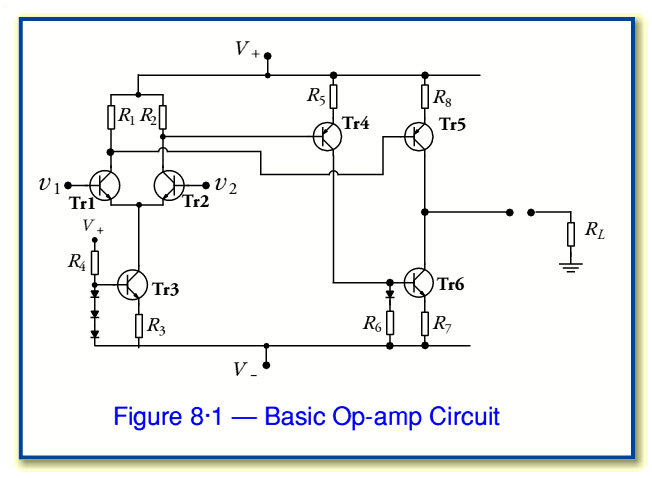
The details of the circuitry inside an op-amp integrated circuit can be very complex, and can vary from type to type, and even from manufacturer to manufacturer. They can also make use of semiconductor effects and constructions that you don’t normally encounter outside of an IC. For clarity, here we will just look at a simplified version of the design. The basic circuit arrangement is shown in figure 8·1.
Tr1/2 form a Long-Tailed Pair differential amplifier for which Tr3 provides a Constant Current source for their common emitters. The input pair drive one of the output transistors (Tr5) directly. The other output transistor (Tr6) is driven via Tr4. Taken together Tr5/6 form a Class A output stage. In this kind of circuit it us usual to have the values chosen so that  and
and  , and to ensure that the transistors have similar gain values. For simplicity we can assume the transistors all have a very high gain so we can treat the base currents as being so small that we can ignore them and assume they are essentially zero. We can therefore understand how the system works as follows:
When the two input are the same (i.e. when  ) the currents through
  and
and  will be the same – each will pass an emitter and collector current of approx
  . This means that the current levels on the two transistors, Tr4 and Tr5, will be almost identical. Since the same current flows though
  and
and  it follows that the value of the potential difference across
  is the same as that across
  . Now the diode in series with
  means that the voltage applied to the base of Tr6 is one junction-drop higher than the potential at that end of the resistor. This counters the voltage drop between the base and emitter of Tr6. Hence the potential across
  is the same as that across
  . i.e. we find that the potential across
  equals that across
  .
.
In effect, the result of the above is that the potential across  (and hence the current that Tr6 draws) is set by the current through
  . Similarly, the potential across
  (and hence the current provided by Tr5) is set by the current through
  . When
  the currents through Tr5 and Tr6 are the same. As a result when we connect a load we find that no current is available for the load, hence the amplifier applies no output voltage to the load,
  .
.
However, if we now alter the input voltage so that  we find that the currents through the output devices Tr5 and Tr6 will now try to differ as the system is no longer ‘balanced’. The difference between the currents through Tr5 and Tr6 now flows through the load. Hence an imbalance in the input voltages causes a voltage an current to be applied to the load. The magnitude of this current and voltage will depend upon the gains of the transistors in the circuit and the chosen resistor values. The system acts as a Differential Amplifier. When
  the output will be positive and proportional to
  . When
  the output will be negative but still proportional to
  (which will now be negative).
This form of circuit is quite a neat one in many ways. It acts in a ‘balanced’ manner so that any imbalance in the inputs creates an equivalent imbalance in the output device currents, thus producing an output. Since the operation is largely in terms of the internal currents the precise choice of the power line voltages,  and
and  , doesn’t have a large effect on the circuit’s operation. We just need the power lines levels to be ‘large enough’ for the circuit to be able to work. For this reason typical Op-Amps work when powered with a wide range of power line voltages – typically from a minimum of
  to
to  Volts. In practice this usually means that the output is limited to a range of voltages a few volts less than the range set by the power lines. In most cases
  Volt lines are used, but this isn’t essential in every case.
Due to the way the circuit operates it has a good Common Mode Rejection Ratio (CMRR) – i.e. any common (shared) change in both input levels is largely ignored or ‘rejected’. Most real Op-Amps use many more transistors than the simple example shown in figure 8·1 and hence can have a very high gain. Their operation is otherwise almost the same as you’d expect from the circuit shown. This means they tend to share its limitations. For example, the pure Class A means that there is usually limit to the available output current (double the quiescent level) and that this can be quite small if we wish to avoid having high power dissipation in the Op-Amp. For a typical ‘small signal’ Op-Amp the maximum available output current is no more than a few milliamps, although higher power Op-Amps may include Class AB stages to boost the available current and power.
There are an enormous variety of detailed types of Op-Amp. Many include features like Compensation where an internal capacitance is used to control the open-loop gain as a function of frequency to help ensure stability when feedback is applied between the output and the input(s). This is why common Op-Amp types such as the 741 family have a very high gain at low frequencies (below a few hundred Hertz) which falls away steadily at higher frequencies. Many Op-Amps such as the TL071 family use FET input devices to minimise the required input current level. Although the details of performance vary, they all are conceptually equivalent to the arrangement shown in figure 8·1.